 Image: Rama, Wikimedia Commons, CC BY-SA 3.0 fr
How a scanning tunnelling microscope sees atoms
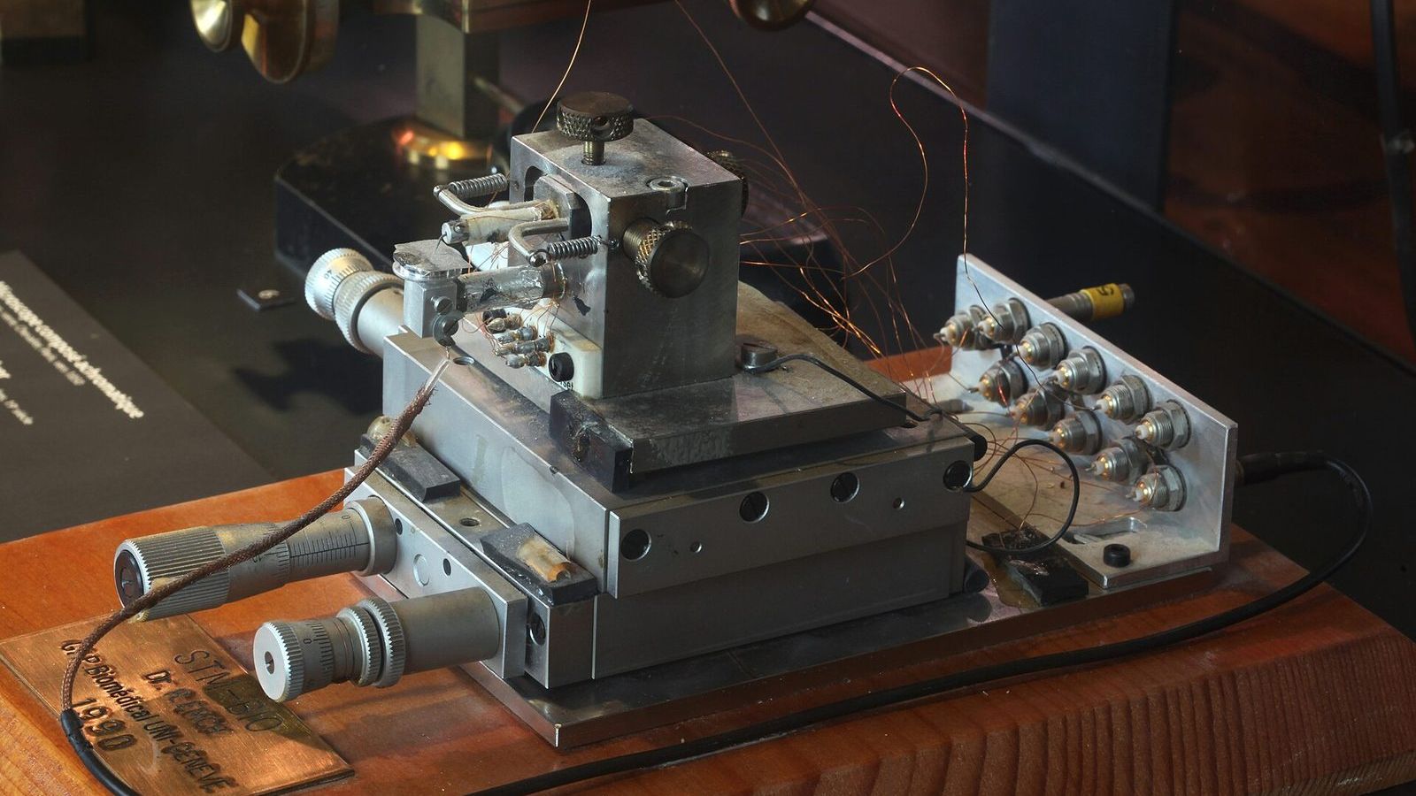
In 1990 Don Eigler and Erhard Schweizer at the IBM Almaden laboratory in California wrote the letters IBM with 35 xenon atoms on a nickel surface, each atom picked up and set down individually. The picture went around the world. The instrument that made it, and that took the picture afterwards, was a scanning tunnelling microscope, invented nine years earlier in Zurich. It has no lens, and it does not use light. It works because electrons can cross a gap they do not have the energy to cross.
The gap
An electron inside a metal is held there by an energy barrier of a few electron volts, the work function. Classically, an electron with less energy than the barrier cannot leave; the surface is a wall. In quantum mechanics the electron's wave function does not stop at the wall. It continues into the forbidden region, decaying exponentially with distance, and if a second piece of metal is brought close enough, the tail of the wave function reaches it. An electron that starts in the first metal has a small probability of being found in the second, and if a voltage is applied between them, a current flows across the vacuum. This is tunnelling, and the current is given by
\[ I \propto V \exp(-2\kappa d), \qquad \kappa = \frac{\sqrt{2 m \phi}}{\hbar}, \]where \(d\) is the width of the gap, \(\phi\) is the work function, and \(m\) is the electron mass. For a typical work function of 4.5 eV, \(\kappa\) is about 11 per nanometre, and \(2\kappa\) is about 22 per nanometre. Increase the gap by one tenth of a nanometre, roughly half the diameter of an atom, and the current drops by a factor of \(e^{2.2}\), which is about 9. Increase it by one nanometre and the current falls by a factor of a few billion.
Turning the exponential into a picture
That steepness is the whole secret. Sharpen a tungsten wire to a point, bring it to within about half a nanometre of a conducting surface, apply a fraction of a volt, and a current of a nanoampere flows. Now move the tip sideways across the surface. Where the surface rises by the height of one atom, the gap shrinks and the current jumps tenfold; where it falls, the current collapses. A feedback circuit moves the tip up and down to keep the current constant, and the record of those movements is a map of the surface with vertical sensitivity of a few picometres, a hundredth of an atom's diameter.
The sideways resolution comes from the same exponential. Even a tip that looks blunt under an ordinary microscope ends, at the atomic scale, in a cluster of atoms, and one of them sits a little lower than the rest. Because the current falls by a factor of 9 for every tenth of a nanometre, almost all of the tunnelling passes through that single lowest atom. The instrument effectively has a probe one atom wide. The tip is moved with piezoelectric crystals, which change their length by a few nanometres per volt, and the whole apparatus is isolated from vibration so that the tip does not crash into the surface it is studying.
Zurich, 1981
Gerd Binnig and Heinrich Rohrer built the first working instrument at the IBM research laboratory in Rüschlikon near Zurich in 1981. Tunnelling across a vacuum gap had been demonstrated before, but nobody had combined it with a scanning tip and a feedback loop, and few believed the vibration problem could be solved. Their first great success came in 1983, when they resolved the arrangement of atoms on the surface of a silicon crystal, a structure called the 7 by 7 reconstruction that had puzzled surface scientists for twenty years. They shared the Nobel Prize in Physics 1986 with Ernst Ruska, who had built the first electron microscope half a century earlier.
Binnig went on to invent the atomic force microscope in 1986, which feels the surface with a tiny cantilever instead of a current and therefore works on insulators as well. Together the two instruments founded the field that came to be called nanotechnology.
What the images show
A tunnelling microscope does not see atoms as little balls. It measures where electrons are available to tunnel at the chosen voltage, which is a map of the electron density near the surface at a particular energy. On a clean metal that map has a bump above each atom, and the picture looks like a close-packed arrangement of spheres. On a semiconductor the bumps can sit between the atoms, or appear and disappear as the voltage is changed, because different electronic states are being probed. Reading the images correctly is a skill, and the first years of the instrument produced some famous misinterpretations.
Used with care, the same microscope measures the energy levels of a single molecule by sweeping the voltage, maps the standing waves of electrons trapped inside a ring of atoms, and watches individual atoms hop across a surface as the temperature rises. The quantum corral images from IBM in 1993, with electron waves rippling inside a circle of 48 iron atoms, are among the most direct pictures of a wave function ever made.
Moving atoms
Eigler's trick in 1990 was to bring the tip closer to a xenon atom until the attraction between them was enough to drag the atom along the surface, then to pull the tip away and leave the atom at its new site. The whole operation was done at 4 kelvin, so that the atoms did not wander off on their own, and the paper in Nature was two pages long. The same technique later built the quantum corral, and in 2013 an IBM team made a stop-motion film, A Boy and His Atom, by moving carbon monoxide molecules frame by frame.
Where else tunnelling appears
The exponential that makes the microscope work governs much else. Alpha decay of nuclei is tunnelling of an alpha particle through the nuclear barrier, and because the probability depends exponentially on the barrier, half-lives range from microseconds to billions of years for nuclei that differ only slightly in energy. Fusion in the Sun's core proceeds by tunnelling of protons through their mutual repulsion at temperatures far too low for a classical collision to succeed. Flash memory stores every bit by tunnelling electrons onto an insulated gate, and the leakage current in modern transistors, whose insulating layers are a few atoms thick, is a tunnelling current that chip designers fight against.
In the Quantum Mechanics Masterclass, Unit 5 solves the barrier problem and derives the exponential above, then applies it to the microscope, to alpha decay, and to the fusion rate of the Sun. The unit's interactive figure lets you change the width and height of a barrier and watch the transmitted wave shrink. It follows Unit 4, where the Schrödinger equation is introduced, and the full sequence is in the curriculum.